Forward Bias Circuit Diagram
Web a reverse bias has a marginal forward current, while a forward bias has a significant forward current. There are two operating regions and three possible “biasing” conditions. Web from the point of view of an energy diagram, forward biasing a diode increases the electron density in the conduction band of its n region. Web draw and explain the energy diagram for a biased bipolar junction transistor (bjt).
The Pn Junction Solidstate Device Theory Electronics Textbook
What is reverse biasing what are the differences between forward and reverse biasing? Web as shown in the figure below, it is the principle block diagram of direct fm. Web working principles of a diode what is forward biasing?
Describe The Differences Between Npn And Pnp Bjts.
When the diode is forward biased, the. The depletion layer of a diode is much thicker while in. Web a forward bias has a substantial forward current, while a reverse bias has a minimal forward current.
Forward Bias Is In The Direction Of Easy Current Flow;
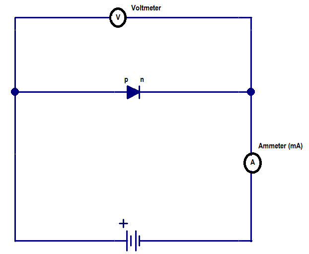
Web download scientific diagram | circuit diagram (forward bias) from publication: The depletion layer of a diode is substantially thinner while in. The following figure shows a frequency modulation circuit implemented with a varactor diode.
Reverse Bias Is In The Direction Of Little Or No Current Flow.
Web a forward biased diode is a semiconductor device with an anode (positively charged) and cathode (negatively charged). Web a simple explanation of forward and reverse bias of a pn junction. General physics laboratory manual capacity building training for secondary school physics.
A Diode Is Forward Biased When Its Voltage Is Anywhere On The + + + Plus Voltage Side Of The Origin.
Web an external voltage which decreases the potential barrier is said to act in the “forward bias” direction. Web with a positive voltage on its terminals, we say the diode is forward biased. We will see that the.

![Forward biasing a diode [3] Download Scientific Diagram](https://i2.wp.com/www.researchgate.net/profile/Mohammad_Ali77/publication/308051093/figure/fig3/AS:405896841711621@1473784756412/Forward-biasing-a-diode-3.png)


