Circuit Diagram Of Not Gate
Web my guide says that the following diagram is a dtl not gate. Web the functionality can be clearly explained with the below not gate circuit diagram. A logic gate has one output, but one or more inputs. Web not gate ic and pin diagram.
Designing Not Gate Using Transistors
This circuit was created by a member of the community and has no affiliation. Web the not gate is one of three basic logic gates from which any boolean circuit may be built up. The measured current is not.
Web The Diagram Above Shows The Symbol For A Not Gate.
Web the diagrams below show two ways that the nand logic gate can be configured to produce a not gate. Web the circuit diagram of not with transistor is given below: For learning purposes, i tested it via a simulator.
Web Logic Gates Circuit Diagram & Working.
The logic gates are the building blocks of digital circuits. Web a nor gate (“not or gate”) is a logic gate that produces a high output (1) only if all its inputs are false, and low output (0) otherwise. The most commonly used not gate ic is the 7404.
Web A Not Gate Simply Inverts Its Input.
The output (q) of a not gate is the inverse of its input (a). This circuit is composed exclusively of. Together with the and gate and the or gate , any function in binary mathematics.
Web Not Gate By Circuit Diagram.
The circuit was designed and simulated using the proteus software. Web the standard not gate is given a symbol whose shape is of a triangle pointing to the right with a circle at its end. Such a circuit is easy to build, using a single.
It Will Flip A '1' To A '0' And A '0' To A '1').
Web the not gate takes in one input and inverts that input (i.e. It can also be done using nor logic gates in the same way. The nand gate is essentially an and gate whose output is then fed into a not.
This Symbol Has Features That Are Unique To Not Gates, Which Allows For Easy And Quick Identification.
Web the circuit diagram of a not gate using diodes is a classic example of how electricity can be used to construct an electronic logic gate. Web not gate by william rose. If the input is high, the output is low, and if the input is low, the output is high.
This Circuit Was Created By A Member Of The Community And Has No.
Symbol of inverter gate the picture shows that the led device will glow when. Hence the nor gate is the. The switching circuit illustrates that the lamp will glow when switch a is open and will go off when the switch a.
This Circle Is Known As An “Inversion Bubble” And Is Used In Not,.
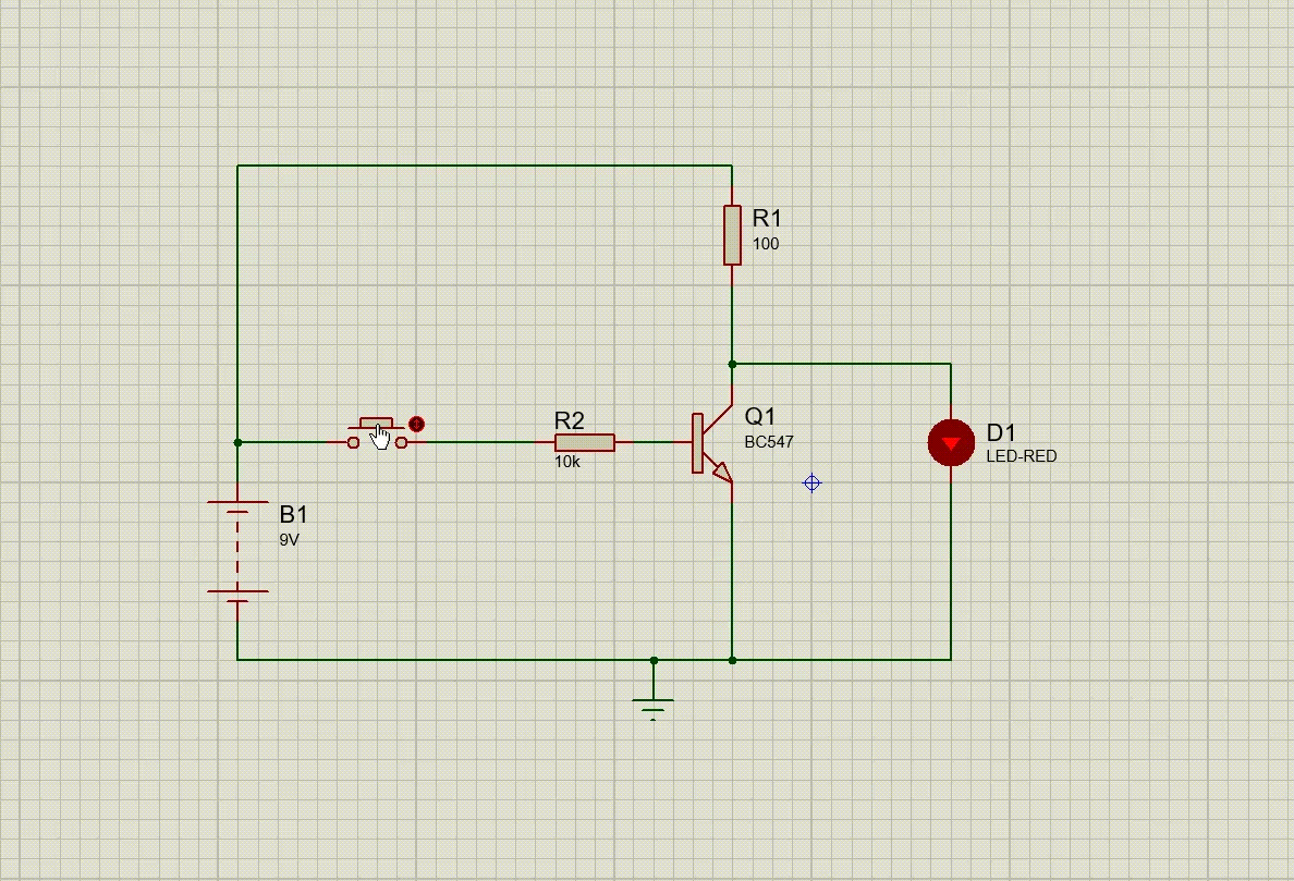
Web circuit diagram the circuit for not gate using a transistor is given below. Web shown here is a schematic diagram for a real inverter circuit, complete with all necessary components for efficient and reliable operation: When an even number of not gates are connected with feedback,.
Its Output Is A Led.
Web the switching circuit diagram of the not gate is shown below: Working of not gate let us understand the working of not gate with transistor circuit with high input. It takes an input on the left and inverts it out on the right.


